Unveiling the Wonders of Single-Sided PCBs: A Journey into Simplicity and Efficiency
In the dynamic realm of electronics, the printed circuit board (PCB) stands as the backbone, orchestrating the intricate dance of electrons that power our modern devices. Among the various types of PCBs, one that has gained prominence for its simplicity and cost-effectiveness is the Single-Sided PCB. In this blog, we’ll embark on a journey to explore the wonders of Single Sided PCB, understanding their structure, applications, advantages, and the impact they’ve had on the world of electronics.
Understanding Single-Sided PCBs:
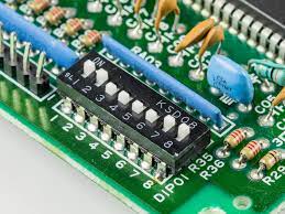
A Single-Sided PCB is characterized by having conductive traces and components on only one side of the board. The other side is typically bare, making it a simpler and more economical option compared to its double-sided and multilayer counterparts. The single layer is usually made of a substrate material, such as fiberglass, with a layer of copper adhered to one side.
Structure and Manufacturing Process:
The manufacturing process of Single-Sided PCBs is relatively straightforward, contributing to their cost-effectiveness. Here’s a brief overview of the key steps:
- Substrate Preparation: The process begins with the selection and preparation of the substrate material. Common materials include fiberglass, phenolic, or a composite material.
- Copper Cladding: A thin layer of copper is then applied to one side of the substrate. This copper layer serves as the conductive pathway for the electronic components.
- Photoresist Application: A layer of photoresist material is applied to the copper-clad substrate. This material is photosensitive and will undergo changes when exposed to light.
- Exposure and Development: The PCB is then exposed to ultraviolet (UV) light through a mask or phototool. The areas covered by the mask will remain protected, while the exposed areas undergo a chemical change. After exposure, the board is developed to remove the unexposed photoresist, leaving behind the desired pattern.
- Etching: The exposed copper is etched away using a chemical solution, leaving behind the conductive traces based on the pattern defined by the photoresist.
- Component Attachment: Electronic components are then attached to the conductive side of the board, using soldering techniques.
Applications of Single-Sided PCBs:
- Consumer Electronics: Single-Sided PCBs find extensive use in various consumer electronics, including calculators, remote controls, and basic electronic devices.
- LED Lighting: The simplicity and cost-effectiveness of Single-Sided PCBs make them suitable for LED lighting applications, where space is limited, and cost considerations are crucial.
- Automotive Electronics: Single-Sided PCBs are employed in various automotive applications, such as dashboard controls, sensors, and entertainment systems.
- Educational Projects: Due to their simplicity and ease of handling, Single-Sided PCBs are often used in educational settings for electronics projects and prototyping.
Advantages of Single-Sided PCBs:
- Cost-Effective: The manufacturing process of Single-Sided PCBs is less complex, resulting in lower production costs.
- Simplicity: With fewer layers and components on a single side, Single-Sided PCBs are easier to design and troubleshoot.
- Suitable for Low-Density Designs: Applications with low component density and simple circuitry benefit from the use of Single-Sided PCBs.
- Rapid Prototyping: Single-Sided PCBs are ideal for rapid prototyping due to their simplicity and quick manufacturing process.
Conclusion:
As we delve into the world of Single-Sided PCBs, it becomes apparent that simplicity can be a powerful design principle. These boards have left an indelible mark on the electronics industry, offering an economical and efficient solution for a myriad of applications. Whether in consumer electronics, lighting, automotive systems, or educational endeavors, Single-Sided PCBs continue to play a vital role in shaping the landscape of modern technology.