Unraveling the Wonders of Double-Sided PCBs: A Deep Dive into Cutting-Edge Electronics
In the ever-evolving realm of electronics, innovation is the key to progress. One such technological marvel that has played a pivotal role in advancing electronic devices is the Double Sided PCB Printed Circuit Board (PCB). This sophisticated piece of engineering has transformed the landscape of electronic design, offering greater flexibility and efficiency in compact spaces. In this blog, we will delve into the intricacies of Double-Sided PCBs, exploring their construction, advantages, applications, and the impact they have on the electronic industry.
Understanding Double-Sided PCBs:
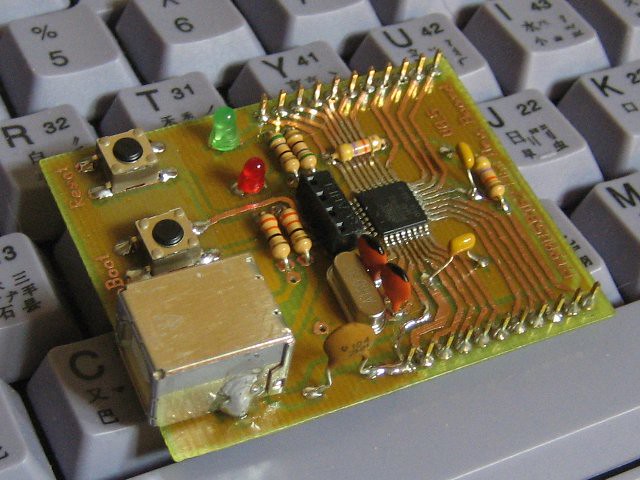
A Printed Circuit Board (PCB) serves as the backbone of electronic devices, providing a platform for interconnecting various components. A Double-Sided PCB, as the name suggests, features conductive traces and components on both sides of the board. This dual-layer configuration significantly enhances the board’s functionality and versatility.
Construction:
The construction of a Double-Sided PCB involves the layering of two separate copper-clad substrates with an insulating material, often referred to as the core. The layers are then laminated together, creating a robust and compact structure. The conductive traces, which form the circuit pathways, are etched onto both sides of the board, allowing for increased component density and intricate circuitry.
Advantages of Double-Sided PCBs:
- Increased Component Density: The dual-layer design of Double-Sided PCBs allows for a higher density of electronic components. This is especially beneficial in applications where space is a premium, enabling engineers to design more compact and efficient devices.
- Enhanced Signal Integrity: With components on both sides of the board, signal paths can be optimized, reducing the risk of signal interference and ensuring better overall signal integrity. This is crucial for high-performance electronic applications.
- Improved Thermal Management: Double-Sided PCBs offer better thermal dissipation due to the increased surface area. This is particularly advantageous in applications where heat management is critical, such as in power electronics and LED lighting.
- Cost-Effectiveness: Despite their advanced design, Double-Sided PCBs can often be more cost-effective than their multilayer counterparts. This makes them an attractive choice for a wide range of electronic applications.
Applications:
Double-Sided PCBs find applications in a myriad of industries, including but not limited to:
- Consumer Electronics: Mobile phones, cameras, and portable devices often utilize Double-Sided PCBs to achieve compact designs without compromising on functionality.
- Industrial Electronics: Automation and control systems benefit from the increased component density and reliability of Double-Sided PCBs.
- Medical Devices: Compact and reliable circuitry is crucial in medical devices, making Double-Sided PCBs an ideal choice for applications such as diagnostic equipment and monitoring devices.
- Automotive Electronics: In the automotive industry, where space is limited and durability is paramount, Double-Sided PCBs are commonly employed in various electronic control units.
Conclusion:
Double-Sided PCBs represent a technological leap in the world of electronics, offering a perfect blend of efficiency, compact design, and cost-effectiveness. As technology continues to advance, these versatile circuit boards will undoubtedly play a central role in shaping the future of electronic devices across various industries. Embracing the capabilities of Double-Sided PCBs opens the door to endless possibilities, paving the way for smaller, more powerful, and intricately designed electronic innovations.