Exploring the Advancements in Electronics: The Marvels of Double-Sided PCBs
In the ever-evolving world of electronics, the backbone of innovation lies in printed circuit boards (PCBs). These crucial components serve as the foundation for electronic devices, facilitating the seamless flow of signals and power. One significant breakthrough in PCB technology is the advent of Double Sided PCB. This innovation has revolutionized the design and functionality of electronic devices, offering enhanced performance and versatility.
Understanding Double-Sided PCBs:
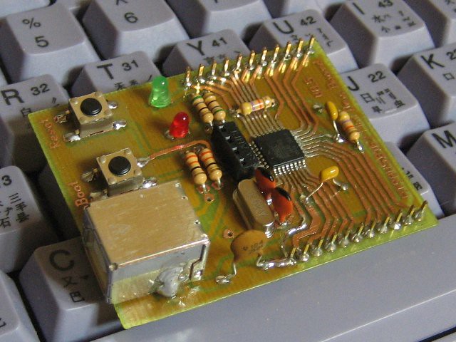
A double-sided PCB, also known as a double-layer PCB, is a type of circuit board that features conductive pathways on both sides of the board. Unlike traditional single-sided PCBs, which have components and traces on only one side, double-sided PCBs utilize both the top and bottom surfaces, effectively doubling the available space for components and traces.
Advantages of Double-Sided PCBs:
- Increased Component Density: One of the primary advantages of double-sided PCBs is their ability to accommodate a higher density of electronic components. With two layers available for placing components and traces, designers can achieve greater functionality in a compact space. This is particularly crucial in modern electronic devices where miniaturization is a key design consideration.
- Enhanced Signal Integrity: The presence of multiple layers allows for better signal routing and minimizes the chances of signal interference. This is especially beneficial for complex electronic systems where signal integrity is critical for optimal performance. The separation of signal and power traces on different layers helps reduce crosstalk and electromagnetic interference.
- Improved Thermal Management: Double-sided PCBs offer better thermal dissipation compared to their single-sided counterparts. The additional layer provides a larger surface area for heat to dissipate, preventing the overheating of sensitive components. This is particularly important in high-performance electronic devices where thermal management is a significant concern.
- Design Flexibility: The dual-layer configuration provides designers with increased flexibility in routing traces and placing components. This flexibility allows for more intricate and efficient circuit designs, leading to improved overall system performance. Designers can implement complex interconnections without compromising the overall layout.
Applications of Double-Sided PCBs:
- Consumer Electronics: Double-sided PCBs are widely used in consumer electronics such as smartphones, tablets, and digital cameras. The compact nature of these devices demands a high component density, and double-sided PCBs fulfill this requirement admirably.
- Automotive Electronics: In the automotive industry, where space is often limited, double-sided PCBs find applications in various electronic control units (ECUs), infotainment systems, and engine control modules. The improved thermal performance is especially beneficial in the challenging environment of a vehicle.
- Industrial Control Systems: Industrial applications often require robust and reliable electronic systems. Double-sided PCBs are employed in industrial control systems, providing the necessary density for complex control circuitry.
Conclusion:
Double-sided PCBs have emerged as a cornerstone in the progression of electronics, contributing significantly to the miniaturization and performance enhancement of electronic devices. Their versatility, enhanced design capabilities, and thermal management features make them a preferred choice in various industries. As technology continues to advance, the role of double-sided PCBs in shaping the future of electronic innovation is poised to become even more pronounced.