Navigating the World of PCB Manufacturing: From Concept to Creation
Printed Circuit Boards (PCBs) form the backbone of modern electronics, serving as the vital link between components, ensuring seamless connectivity and functionality. Behind every electronic device lies a meticulously crafted PCB, and understanding the intricacies of PCB manufacturer sheds light on the technological marvels we use daily.
Chapter 1: The Basics of PCBs
Before delving into the manufacturing process, it’s essential to grasp the basics of what a PCB is. A PCB is a flat board made of non-conductive material, typically fiberglass, that supports and connects various electronic components through conductive pathways etched onto the surface. These pathways are usually made of copper, forming a network of traces that allow the flow of electricity.
Chapter 2: Designing the Blueprint
The journey of a PCB begins with its design. Engineers and designers use specialized software to create a blueprint that outlines the placement of components, the routing of traces, and other crucial details. This design serves as the guiding document for the manufacturing process.
Chapter 3: Material Matters
The choice of materials plays a pivotal role in the manufacturing of PCBs. The most common material for the substrate is fiberglass, but other options include materials like ceramic and metal-core boards for specific applications. The conductive traces are usually made of copper, with the thickness of the copper layers determined by the intended use and required electrical characteristics of the PCB.
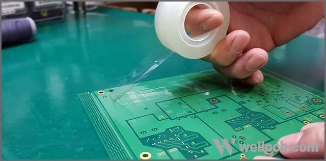
Chapter 4: Etching and Layering
Once the design and materials are finalized, the manufacturing process kicks into high gear. A thin layer of copper is laminated onto the substrate, and the excess copper is etched away, leaving behind the desired traces. For multi-layered PCBs, several layers are stacked and bonded together. This layering process allows for complex and compact designs, common in advanced electronic devices.
Chapter 5: Drilling and Plating
Next comes the drilling of holes for component placement and interconnecting the layers. The holes are then plated with a conductive material to establish electrical connections between different layers. This step is crucial for ensuring the PCB can support the desired circuitry and functionality.
Chapter 6: Soldering Components
With the holes drilled and plated, it’s time to populate the PCB with electronic components. Automated machines or skilled technicians carefully place and solder components onto the board. Surface Mount Technology (SMT) and Through-Hole Technology (THT) are the two primary methods used for component mounting, with SMT being more prevalent in modern electronics due to its efficiency and space-saving advantages.
Chapter 7: Quality Control
Quality control is a critical aspect of PCB manufacturing. Rigorous testing ensures that each board meets the required specifications and can withstand the demands of its intended application. Advanced testing techniques, such as Automated Optical Inspection (AOI) and In-Circuit Testing (ICT), help identify defects and ensure the highest level of reliability.