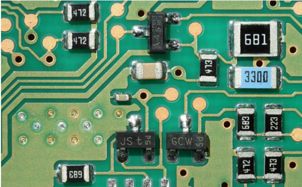
Unraveling the Wonders of Multilayer PCBs: A Deep Dive into Advanced Circuitry
In the ever-evolving landscape of electronics, the demand for smaller, faster, and more efficient devices has led to significant advancements in printed circuit board (PCB) technology. Among these breakthroughs, Multilayer PCBs stand out as a crucial innovation, providing a versatile and compact solution for the intricate circuitry found in modern electronic devices.
Understanding Multilayer PCBs:
A PCB serves as the backbone of electronic devices, providing a platform for the interconnection of various electronic components. Multilayer PCBs take this concept to the next level by incorporating multiple layers of conductive material separated by insulating layers, allowing for a higher density of components and more complex circuit designs.
Key Features and Advantages:
- Space Efficiency: Multilayer PCBs excel in space efficiency, as they allow for the stacking of multiple layers of circuitry. This compact design is crucial for miniaturized devices, where space constraints are a significant concern.
- Increased Component Density: With more layers available for component placement, Multilayer PCBs can accommodate a higher density of electronic components. This facilitates the creation of complex and sophisticated circuits, making them ideal for advanced applications.
- Improved Signal Integrity: The multiple layers in a Multilayer PCB provide a better environment for managing power distribution and minimizing signal interference. This leads to improved signal integrity, reducing the risk of electromagnetic interference (EMI) and signal crosstalk.
- Enhanced Performance: The increased component density and improved signal integrity contribute to enhanced overall performance. Multilayer PCBs are often used in high-frequency applications where signal accuracy and speed are critical.
Design Considerations:
- Layer Stackup: The arrangement of conductive and insulating layers, known as the layer stackup, is a crucial aspect of Multilayer PCB design. Designers carefully plan the stackup to ensure optimal signal integrity, power distribution, and thermal management.
- Routing and Traces: Efficient routing of traces becomes more complex with multilayer designs. Careful consideration must be given to signal paths, power planes, and ground planes to minimize interference and maintain performance.
- Thermal Management: As the component density increases, managing heat becomes essential. Multilayer PCBs often incorporate thermal vias, heat sinks, and strategic placement of components to dissipate heat effectively.
Applications:
Multilayer PCBs find applications across a wide range of industries, including:
- Telecommunications: In devices like smartphones, routers, and communication equipment where space is at a premium, multilayer PCBs enable the integration of complex circuitry.
- Medical Devices: Medical devices, with their intricate electronics and compact designs, benefit from the high-density capabilities of multilayer PCBs.
- Automotive Electronics: In modern vehicles, where electronic control units and sensors play a crucial role, multilayer PCBs ensure efficient space utilization and robust performance.
Conclusion:
Multilayer PCBs represent a pivotal advancement in electronic design, enabling the creation of smaller, more powerful, and efficient devices. As technology continues to push the boundaries of what is possible, the role of multilayer PCBs in shaping the landscape of electronics will undoubtedly become even more significant. With their ability to support complex circuitry, enhance performance, and meet the demands of diverse industries, multilayer PCBs stand as a testament to the relentless pursuit of innovation in the field of electronics.
